- 您现在的位置:买卖IC网 > Sheet目录2004 > LTC1745CFW#TRPBF (Linear Technology)IC ADC 12BIT 25MSPS LN 48TSSOP
4
LTC1745
1745f
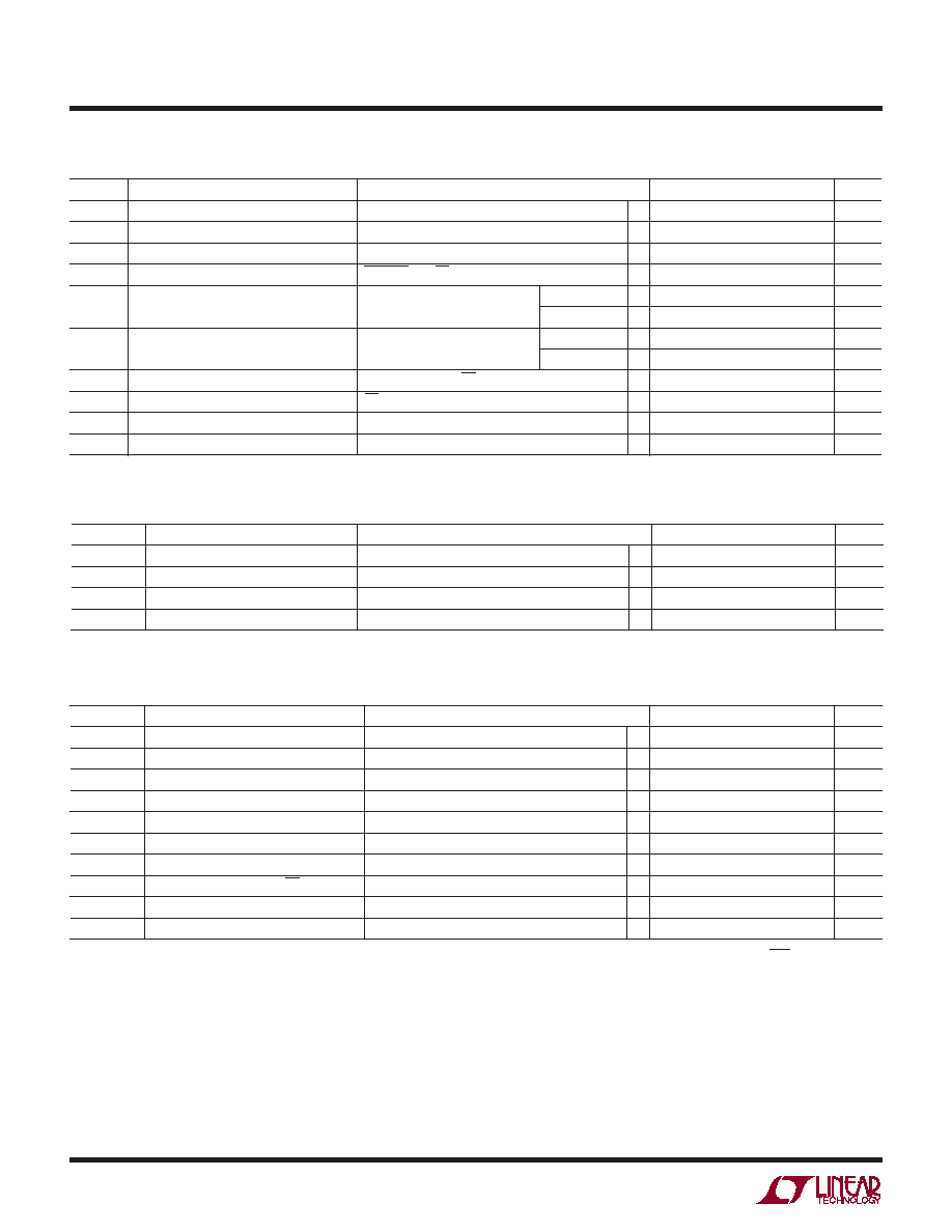
SYMBOL
PARAMETER
CONDITIONS
MIN
TYP
MAX
UNITS
VDD
Positive Supply Voltage
4.75
5.25
V
IDD
Positive Supply Current
2V Range, Full-Scale Input
q
76
91
mA
PDIS
Power Dissipation
2V Range, Full-Scale Input
q
380
455
mW
OVDD
Digital Output Supply Voltage
0.5
VDD
V
SYMBOL
PARAMETER
CONDITIONS
MIN
TYP
MAX
UNITS
fSAMPLE
Sampling Frequency
(Note 9)
q
1
25
MHz
t1
ENC Low Time
(Note 9)
q
19
20
1000
ns
t2
ENC High Time
(Note 9)
q
19
20
1000
ns
t3
Aperture Delay of Sample-and-Hold
0
ns
t4
ENC to Data Delay
CL = 10pF (Note 8)
q
1.4
4
10
ns
t5
ENC to CLKOUT Delay
CL = 10pF (Note 8)
q
0.5
2
5
ns
t6
CLKOUT to Data Delay
CL = 10pF (Note 8)
q
02
ns
t7
DATA Access Time After OE
↓
CL = 10pF (Note 8)
10
25
ns
t8
BUS Relinquish Time
(Note 8)
10
25
ns
Data Latency
5
cycles
The q indicates specifications which apply over the full operating temperature
range, otherwise specifications are at TA = 25°C. (Note 5)
TI I G CHARACTERISTICS
U
W
Note 1: Absolute Maximum Ratings are those values beyond which the life
of a device may be impaired.
Note 2: All voltage values are with respect to ground with GND
(unless otherwise noted).
Note 3: When these pin voltages are taken below GND or above VDD, they
will be clamped by internal diodes. This product can handle input currents
of greater than 100mA below GND or above VDD without latchup.
Note 4: When these pin voltages are taken below GND, they will be
clamped by internal diodes. This product can handle input currents of
>100mA below GND without latchup. These pins are not clamped to VDD.
Note 5: VDD = 5V, fSAMPLE = 25MHz, differential ENC/ENC = 2VP-P 25MHz
sine wave, input range =
±1.6V differential, unless otherwise specified.
Note 6: Integral nonlinearity is defined as the deviation of a code from a
straight line passing through the actual endpoints of the transfer curve.
The deviation is measured from the center of the quantization band.
Note 7: Bipolar offset is the offset voltage measured from – 0.5 LSB
when the output code flickers between 0000 0000 0000 and
1111 1111 1111.
Note 8: Guaranteed by design, not subject to test.
Note 9: Recommended operating conditions.
SYMBOL
PARAMETER
CONDITIONS
MIN
TYP
MAX
UNITS
VIH
High Level Input Voltage
VDD = 5.25V
q
2.4
V
VIL
Low Level Input Voltage
VDD = 4.75V
q
0.8
V
IIN
Digital Input Current
VIN = 0V to VDD
q
±10
A
CIN
Digital Input Capacitance
MSBINV and OE Only
1.5
pF
VOH
High Level Output Voltage
OVDD = 4.75V
IO = –10A
4.74
V
IO = – 200A
q
4V
VOL
Low Level Output Voltage
OVDD = 4.75V
IO = 160A
0.05
V
IO = 1.6mA
q
0.1
0.4
V
IOZ
Hi-Z Output Leakage D11 to D0
VOUT = 0V to VDD, OE = High
q
±10
A
COZ
Hi-Z Output Capacitance D11 to D0
OE = High (Note 8)
q
15
pF
ISOURCE
Output Source Current
VOUT = 0V
– 50
mA
ISINK
Output Sink Current
VOUT = 5V
50
mA
The q indicates specifications which apply over the full
operating temperature range, otherwise specifications are at TA = 25°C. (Note 5)
DIGITAL I PUTS A D DIGITAL OUTPUTS
U
The q indicates specifications which apply over the full operating temperature
range, otherwise specifications are at TA = 25°C. (Note 5)
POWER REQUIRE E TS
W
U
发布紧急采购,3分钟左右您将得到回复。
相关PDF资料
LTC1746IFW#TRPBF
IC ADC 14BIT 25MSPS LP 48TSSOP
LTC1747IFW#PBF
IC ADC 12BIT 80MSPS 48-TSSOP
LTC1748CFW#TRPBF
IC ADC 14BIT 80MSPS 48-TSSOP
LTC1749IFW#PBF
IC ADC 12BIT 80MSPS SMPL 48TSSOP
LTC1750IFW#PBF
IC ADC 14BIT 80MSPS SMPL 48TSSOP
LTC1799HS5#TRPBF
IC OSC SILICON 33MHZ TSOT23-5
LTC1821ACGW
IC D/A CONV 16BIT PRECISE 36SSOP
LTC1851CFW
IC ADC 12BIT 1.25MSPS 48-TSSOP
相关代理商/技术参数
LTC1745IFW
功能描述:IC ADC SMPL 12BIT 25MSPS 48TSSOP RoHS:否 类别:集成电路 (IC) >> 数据采集 - 模数转换器 系列:- 标准包装:1,000 系列:- 位数:12 采样率(每秒):300k 数据接口:并联 转换器数目:1 功率耗散(最大):75mW 电压电源:单电源 工作温度:0°C ~ 70°C 安装类型:表面贴装 封装/外壳:24-SOIC(0.295",7.50mm 宽) 供应商设备封装:24-SOIC 包装:带卷 (TR) 输入数目和类型:1 个单端,单极;1 个单端,双极
LTC1745IFW#PBF
功能描述:IC ADC 12BIT 25MSPS LN 48TSSOP RoHS:是 类别:集成电路 (IC) >> 数据采集 - 模数转换器 系列:- 标准包装:1,000 系列:- 位数:12 采样率(每秒):300k 数据接口:并联 转换器数目:1 功率耗散(最大):75mW 电压电源:单电源 工作温度:0°C ~ 70°C 安装类型:表面贴装 封装/外壳:24-SOIC(0.295",7.50mm 宽) 供应商设备封装:24-SOIC 包装:带卷 (TR) 输入数目和类型:1 个单端,单极;1 个单端,双极
LTC1745IFW#TR
功能描述:IC ADC SMPL 12BIT 25MSPS 48TSSOP RoHS:否 类别:集成电路 (IC) >> 数据采集 - 模数转换器 系列:- 标准包装:1,000 系列:- 位数:12 采样率(每秒):300k 数据接口:并联 转换器数目:1 功率耗散(最大):75mW 电压电源:单电源 工作温度:0°C ~ 70°C 安装类型:表面贴装 封装/外壳:24-SOIC(0.295",7.50mm 宽) 供应商设备封装:24-SOIC 包装:带卷 (TR) 输入数目和类型:1 个单端,单极;1 个单端,双极
LTC1745IFW#TRPBF
功能描述:IC ADC 12BIT 25MSPS LN 48TSSOP RoHS:是 类别:集成电路 (IC) >> 数据采集 - 模数转换器 系列:- 标准包装:1,000 系列:- 位数:12 采样率(每秒):300k 数据接口:并联 转换器数目:1 功率耗散(最大):75mW 电压电源:单电源 工作温度:0°C ~ 70°C 安装类型:表面贴装 封装/外壳:24-SOIC(0.295",7.50mm 宽) 供应商设备封装:24-SOIC 包装:带卷 (TR) 输入数目和类型:1 个单端,单极;1 个单端,双极
LTC1746CFW
功能描述:IC ADC 14BIT 25MSPS LP 48TSSOP RoHS:否 类别:集成电路 (IC) >> 数据采集 - 模数转换器 系列:- 标准包装:1,000 系列:- 位数:12 采样率(每秒):300k 数据接口:并联 转换器数目:1 功率耗散(最大):75mW 电压电源:单电源 工作温度:0°C ~ 70°C 安装类型:表面贴装 封装/外壳:24-SOIC(0.295",7.50mm 宽) 供应商设备封装:24-SOIC 包装:带卷 (TR) 输入数目和类型:1 个单端,单极;1 个单端,双极
LTC1746CFW#PBF
功能描述:IC ADC 14BIT 25MSPS LP 48TSSOP RoHS:是 类别:集成电路 (IC) >> 数据采集 - 模数转换器 系列:- 标准包装:1 系列:microPOWER™ 位数:8 采样率(每秒):1M 数据接口:串行,SPI? 转换器数目:1 功率耗散(最大):- 电压电源:模拟和数字 工作温度:-40°C ~ 125°C 安装类型:表面贴装 封装/外壳:24-VFQFN 裸露焊盘 供应商设备封装:24-VQFN 裸露焊盘(4x4) 包装:Digi-Reel® 输入数目和类型:8 个单端,单极 产品目录页面:892 (CN2011-ZH PDF) 其它名称:296-25851-6
LTC1746CFW#TR
功能描述:IC ADC SMPL 14BIT 25MSPS 48TSSOP RoHS:否 类别:集成电路 (IC) >> 数据采集 - 模数转换器 系列:- 标准包装:1,000 系列:- 位数:12 采样率(每秒):300k 数据接口:并联 转换器数目:1 功率耗散(最大):75mW 电压电源:单电源 工作温度:0°C ~ 70°C 安装类型:表面贴装 封装/外壳:24-SOIC(0.295",7.50mm 宽) 供应商设备封装:24-SOIC 包装:带卷 (TR) 输入数目和类型:1 个单端,单极;1 个单端,双极
LTC1746CFW#TRPBF
功能描述:IC ADC 14BIT 25MSPS LP 48TSSOP RoHS:是 类别:集成电路 (IC) >> 数据采集 - 模数转换器 系列:- 标准包装:1,000 系列:- 位数:12 采样率(每秒):300k 数据接口:并联 转换器数目:1 功率耗散(最大):75mW 电压电源:单电源 工作温度:0°C ~ 70°C 安装类型:表面贴装 封装/外壳:24-SOIC(0.295",7.50mm 宽) 供应商设备封装:24-SOIC 包装:带卷 (TR) 输入数目和类型:1 个单端,单极;1 个单端,双极